For part 1 of the Digital VFO click here.
For part 2 of the Digital VFO click here.
Digital VFO & RF Oscillator Module
"For the G6LBQ Irwell HF Transceiver"
Welcome to part 3 of my blog post series in which I present details of the hardware for my Digital VFO and RF oscillator module. This is a significant building block for the “Irwell HF Transceiver" project and I Present my buffer amplifiers for the SI5351 ICs and design a PCB to produce a completed working module.
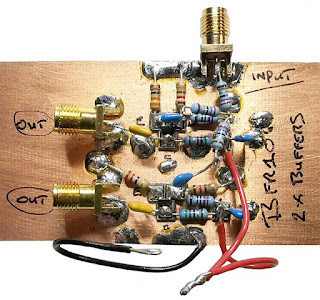 | ||
| My prototype SI5351 buffer & signal splitter circuit! | |
When I set out on my journey to develop and build the “Irwell HF Transceiver” a decision was made to adopt a modular construction approach, my rational being that the transceiver could evolve over time with improvements and upgrades. The modular approach also helps to simplify what is actually a complex project and it paves the way in establishing a useful set of modules that can be utilized in other projects.
When designing and developing the modules, a degree of foresight is needed to determine how the various modules will interconnect and as I have discovered, failure to get this right can be costly and set the project back.
The digital VFO and oscillator is one such module where foresight is needed, as it will be used for both the receiver and transmitter as well as providing control for switching filters, signal paths and more. For now I am concentrating all of my efforts on the receiver modules and will add the transmitter modules later.
"In effect I am building a multi-mode HF communication receiver that can be upgraded to a transceiver at a later date if desired."
My approach has the benefit of providing me with a high performance receiver that I can listen to and enjoy whilst working on the modules that will later form the transmit side.
For now I plan to use separate RF mixer circuits for the receiver and transmitter stages, this will simplify signal routing and provide possibilities for split frequency or split band operation. The use of independent RX/TX mixers does, however, mean that signals from the VFO and oscillator module will either have to be switched between modules or buffered and split.
Splitting the VFO and oscillator signals will require a total of six buffer circuits, two for the VFO, two for the BFO and two for the 2nd conversion oscillator (for when the receiver gets updated to a dual conversion superhet). This is the option I have chosen, as it provides a convenient way to control the signal level provided to each of the mixer, demodulator and modulator circuits.
Some may find my approach a bit excessive and a poor use of resources but as it is not a commercial product, I say, "to hell with the expense".
For the buffer stages, I designed a simple common collector amplifier circuit that is biased directly from the Si5351 clock output. The circuit diagram below shows a pair of the buffer circuits that split the source signal into two paths. RF out 1 and RF out 2.
I used high linearity low noise BFR106 RF transistors for the buffers as they are current and readily available. The devices are supplied in a surface mount SOT23 package and their specifications make them an ideal device for ham radio projects.
From the above circuit, it can be seen that PI resistor attenuators are present in the transistor emitter legs. This establishes an impedance match of 50 ohms to the preceding stage as well as defining the output signal amplitude. The PI network resistor values are simply reconfigured for each of the buffer circuits so that the correct level of the signal is provided at the output and proceeding stage. With the PI values shown, the output signal measured on my home-brew digital RF power meter is +7dbm, ideal for diode ring mixers.
Using the criteria I have outlined, my VFO oscillator module contains three SI5351 clock generators and a total of six RF buffer stages. These can be individually configured to provide a signal level that is sufficient for driving most RF mixers, modulators and demodulator circuits.
Now that the salient points of the VFO and oscillator have been covered, we can now move onto the schematic diagrams and hardware. The project has been divided into three sections with a schematic diagram drawn up for each one.
Please note that the schematic diagrams presented on the blog have been compressed to improve page loading times. This does reduce the overall image quality but is a necessary compromise for the web. Higher-resolution schematics will be made available to download from my Groups.io community group once I have finished documenting the VFO and oscillator section in part 4.
Here is the schematic diagram for the microcontroller board, which also contains the function buttons and a TFT display:
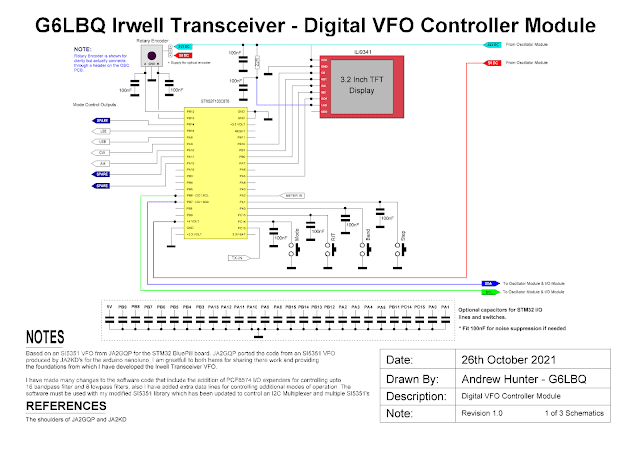 |
| Click to enlarge to full size! |
Next is the schematic diagram for the I2C multiplexer, the SI5351 oscillators and the splitter buffer circuits:
 |
| Click to enlarge to full size! |
Note I have used individual 25 MHz clock crystals for each of the Si5351 devices, it may be more beneficial to use a single precision TCXO oscillator.
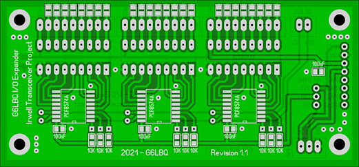
And finally here is the schematic diagram for the I/O expander:
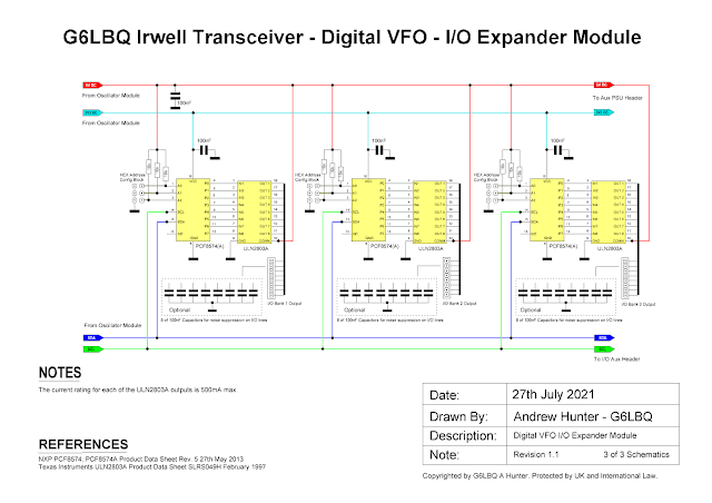 |
| Click to enlarge to full size! |
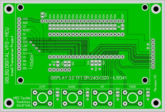
Three PCBs have been designed for the VFO and oscillator module that conveniently connect and stack together. My intention is to keep the digital electronics together and away from the analogue RF circuits, thus avoiding unwanted interference between the two. The digital electronics will be mounted behind the transceivers front panel in a screened cavity away from everything else.
All of the printed circuit boards are double sided with components mounted on both sides. This helps to reduce the size of the PCBs and reduce production costs.




all points noted Andy C U S, F
ReplyDeleteLovely Project , Am on it ! Cheers , AP2RF
ReplyDelete