In this blog post I bring some of the completed "Irwell HF Transceiver" modules together and consolidate them on to a single PCB.
When I started on my journey to build a high-performance HF transceiver (AKA Irwell) I had no idea as to what the final architecture would consist of, I knew of the basic stages required to build a transceiver but I had no grand plan as to what the various stages would consist of. My approach was defined around building individual modules so I could experiment and learn along the way, finished modules then slot together kind of like a jigsaw puzzle!
My cavalier approach led me to build many different modules, some were good and some were bad but the beauty of my approach meant that modules or stages could be changed or improved as the project evolved.
So far, my journey has been an immense amount of fun and provided me a lot of satisfaction along the way. I have built and changed many modules in my pursuit of performance and greatness to the point I believe there is little or no room for improvement.
I have spent some time reflecting on what I have achieved to date and how best to move the project forward. The receiver side of the project is complete so I now need to push forward with the development of the transmitter stages.
In February 2022 I developed a transmitter modulator suitable for SSB, AM and CW modes, this module was, in fact, my first module for the "Irwell" transmit chain.
Click here to take a look at the transmit modulator module
The next logical step is to feed the TX modulator through a set of mixer stages and generate the transmit signals and to do this, I have decided to share the two H-Mode mixers used in the receiver section. Before I get into the nuts & bolts of this, I want to take the opportunity to touch on a few areas of the project that have evolved before I consolidate some of my existing modules onto a single PCB.
My transceiver project started out as a single conversion superhet, though I always wanted it to be a dual conversion arrangement so I could enjoy general coverage receive across the whole HF spectrum. Dual conversion makes this possible by keeping unwanted mixer products above the wanted receive spectrum and placing them above the highest receive frequency, which is 30 MHz.
Early on in development, dual conversion was not possible due to a lack of software available to programme the various oscillators required for this architecture. I am not a software engineer per se but a mere dabbler so writing the software from scratch was a daunting task and beyond my abilities. Instead I turned to the internet and found many examples of code, though all were written for a single conversion.
For some time I used a software sketch sourced from JA2GQP and JA2NKD and ran the transceiver as a single conversion type. This worked well and I was able to make many changes to the software to support my hardware as the project evolved. Ultimately the holy grail was to have my own software to achieve dual conversion status and thanks to my dear friend Dave, this has been made possible... Thanks Dave 👍
Dual conversion requires some hardware changes that I have not previously covered on the blog. These include the addition of a roofing filter, a 2nd mixer stage, and a post mixer amplifier stage. The second mixer stage is a duplicate of the first, which I previously blogged about so there is no point in going over this again here.
Click here to take a look at my H-Mode mixer module.
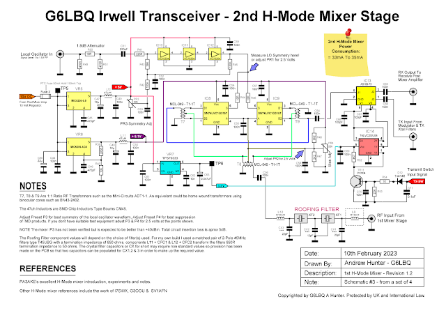
The Roofing Filter I sourced has four poles and is based on a matched pair of 45 MHz two pole filters manufactured by Tellurian part number T45U15BG. The specifications are as follows:
- -3db Bandwidth Is +/- 7.5 KHz
- Termination Impedance 650 Ohms.
- Termination Capacitance 3pF.
- Ripple 1dB Max
- Insertion Loss 3dB Max
In order to transform the filter's input & output impedance from 650 ohms to 50 ohms, I calculated the component values for an LC matching network and built up the following circuit as a prototype:
For the 610nH inductors, I wound 13 turns of 0.25mm enamelled copper wire on T37-6 iron cores. The prototype filter was hooked up to my spectrum analyser and the end result is shown in the scan below:
As can be seen from the spectrum analyser scan, the filter looks excellent and I am very happy with the shape and low insertion loss.
With the progression to dual conversion, the losses in the receive chain start to increase so to mitigate this, some post mixer amplification is required. The losses in the receive chain prior to reaching the main xtal filters and subsequent IF amplification are as follows:
- Front End Bandpass filters 1.5dB or less
- H-Mode Mixer #1 -5dB
- H-Mode Mixer #2 -5dB
- 45 MHz Roofing Filter -2.88dB
The total loss of these four stages is -14.3 dB
A post mixer amplifier with 14dB gain was developed and is presented in the schematic below:
 |
| Click to enlarge full size for clarity! |
Next is an image of the prototype amplifier built "Dead Bug" fashion on a scrap piece of copper clad PCB material:
As I mentioned earlier in this blog post, there are now two H-Mode mixers in the transceiver and these require a means of switching the signal path between receive and transmit modes. For this job I opted for solid state switching using low-cost AS169-73LF SPDT RF Switches manufactured by Skyworks . These are PHEMT GaAs devices in an ultraminiature SOT-6 package and feature some really nice specifications:
- 300 kHz to 2.5GHz Frequency operation
- Low DC Power Consumption
- Low Insertion Loss 0.3 dB to 0.5 dB Maximum
- Low DC Power Consumption
- IP3 52 dBm Typical
 |
| Device Pinout |
As can be seen from the above pinout diagram, the device is controlled via Pin 4 -V1 and Pin 6 -V2.
 |
| Truth Table |
The truth table outlines the switching of V1 and V2 and the switching relationship with J1-J2 and J1-J3. I used a 74LVC2GU04 dual unbuffered inverter to toggle the V1 & V2 control lines of the AS16973LF.
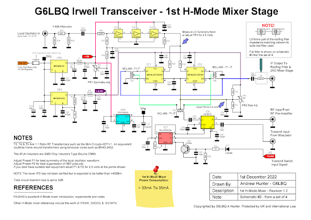
For clarity I have produced a separate circuit diagram for each of the revised mixer stages that shows the inclusion of the RF switches.
 | ||||
| Click to enlarge full size for clarity! |
 |
| Click to enlarge full size for clarity! |
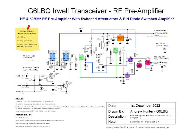
The last module to receive a small hardware change was the receive RF Preamplifier. I added a couple of additional 2N7002 transistors to the switching logic so the preamplifier could be controlled (switched in or out) using just one I/O pin from the VFO/MCU module as opposed to the previous two.
The STM32 BluePill microcontroller board has 37 general I/O pins but due to the complexity of my project, this amount is insufficient. More I/O pins can be made available by using I/O expanders, which is what I have done. My VFO module comprises of three stacked PCB's, one for the Display & MCU, one for the Oscillators and finally one for I/O expansion. The I/O expander PCB contains three PCF8574 IC's which, in turn, provide a further 24 I/O pins. Despite the addition of more I/O pins, I still did not have enough to support all of my hardware; hence the hardware changes to the RF Preamplifier.
The schematic for the revised receive RF Preamplifier is shown below:
 |
| Click to enlarge full size for clarity! |
To summarize, the following changes have been made:
- Post Mixer Amplifier developed.
- 45MHz Roofing filter developed.
- H-Mode Mixer reworked to include RX/TX switching.
- Receive RF Preamplifier modified for single I/O pin on/off operation.
- Update schematic diagrams
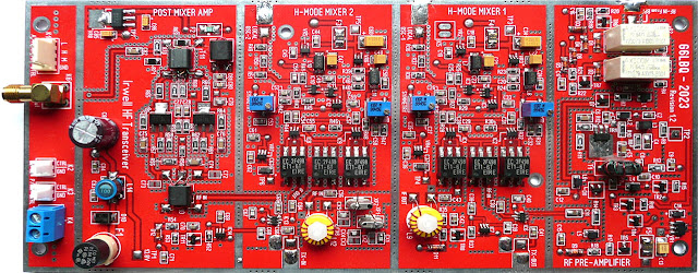
All of the above have now been consolidated onto a single PCB and a schematic diagram set produced based on those presented in this blog post. The NEW consolidated PCB was built and has been in daily use on receive for several months without any issues.
Here is the consolidated PCB that shares the same footprint as my "Band-Pass Filter PCB" and can therefore be stacked.
 |
| Click to enlarge full size for clarity! |
I will be adding some screening around the perimeter of the board and also between the various stages. The PCB has tinned areas ready to take screening material which will also serve as a means of enclosing the board and provide overall shielding.
The work carried to produce this module has certainly tidied things up and set the foundations for the transmitter side of the project, I now feel there is light at the end of the tunnel and, pending no unforeseen issues, the remaining modules should be relatively straightforward to produce.
In my next blog post, I will present the NEW VFO software as well as detailing some changes that have been made to the associated hardware.
Project files will be made available via the Groups.io platform by joining my G6LBQ community group, where you can discuss my projects, ask questions and help others.


No comments:
Post a Comment
I appreciate your comments on the blog content, however the blog has been subject to idiots trying to use the comments facility as a means to post advertisements & spam so all comments are now approved and moderated.