Here at the G6LBQ ham shack, I have various receivers and radio scanners that I use for monitoring the VHF/UHF ham bands and other RF signals that interest me. In an ideal world, each receiver would have its own dedicated antenna but that is not practical for me so I have decided to design and build an RF Multicoupler.
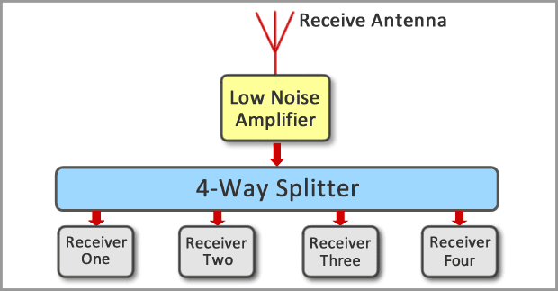
The main application of an RF Multicoupler is to enable multiple receivers to share a common antenna and it does this by splitting the incoming signal into a number of output ports, as illustrated in the image below.
There are two types of RF Multicoupler, Passive and Active, both types incorporate a form of power divider to split the input signal into multiple paths, which introduce inherent losses due to the signal splitting process. The active type has a "Low Noise Amplifier" (LNA) to compensate for the losses, and if required add some additional gain to boost the signal level.
A simple form of RF splitter is the Owen splitter that can be built with resistors. A two-port splitter can be built with just four resistors and a four port with twelve resistors. The downside of the Owen splitter is the overall insertion loss, which runs at 10dB for the 2-port and 20dB for the 4-port.
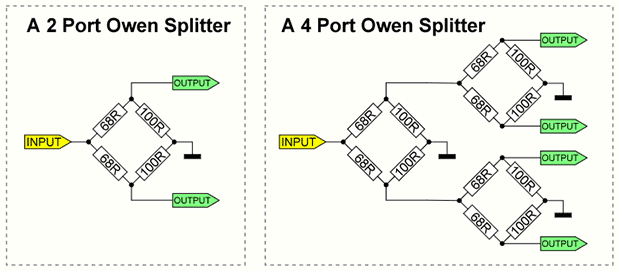 |
50 Ohm 2 & 4 Port Owen Splitters |
The Owen Splitter does have the advantage of being broadband with the only limitation being that of parasitic effects produced by the resistors and associated mounting. That said, the Owen Splitter should be good for several GHz providing care is taken to mount the resistors on a suitable substrate, FR4 PCB material should be okay for up to 1.2GHz but beyond that PTFE PCB should be considered, its dielectric properties are far superior at microwave frequencies.
A more efficient way to split the signal is by using dedicated RF Power Splitters/Combiners, as these are not as lossy and provide greater isolation between the ports.
The "Wilkinson Power Divider" falls into this category and is popular at microwave frequencies, it is built using quarter wave transmission lines that can easily be fabricated as copper tracks on printed circuit boards.
For general HF, VHF and UHF frequencies core and wire-based splitter combiners can be used and either built or purchased from RF specialists.
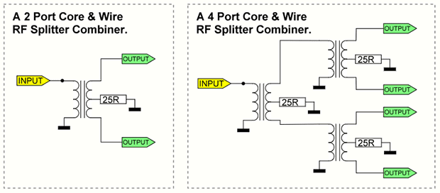 |
50 Ohm - 2 & 4 Port Core & Wire Splitter Combiners |
It should be noted core & wire splitter combiners usually have one or more fixed value tuning capacitors not shown in the above illustration, the purpose of the capacitors is to flatten the frequency response.
With all RF splitters, the more you split the input signal the greater the losses become; this may be acceptable for some applications, such as the distribution of a large signal source, for weaker signals, a "Low Noise Amplifier" should be considered to overcome the losses.
Having considered the options, I am going to build an RF Multicoupler
that will share a single antenna with up to four receivers and incorporate a
low noise RF amplifier. I am interested in receiving signals in the range of 20 to 500MHz so my choice of components in the design will have to be broadband.
Mini Circuits are a well established and global leader in the supply of RF and microwave components and they offer a wide range of RF splitter combiners and low noise amplifiers and are therefore a good choice for sourcing key components. I spent some time looking through the Mini Circuits website and studying various data sheets and decided on the following parts for my project:
- PGA-103+ Low Noise RF Amplifier
- ADP-2-1W Power Splitter Combiners
A schematic for the project was prepared and is shown below.
 |
| Click image to enlarge to full size! |
Next a PCB was designed and the Gerber files sent for manufacturing, the PCB CAD image is shown below.
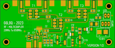 |
| The Actual PCB Size is 90mm by 40mm |
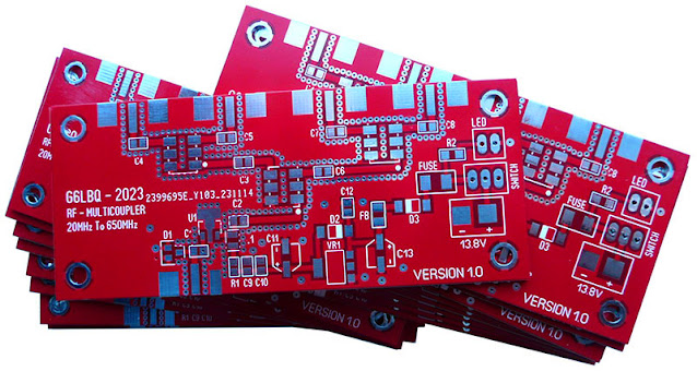
A week after sending the PCB Gerber files for manufacture, I received a batch of 20 boards, which looked great.
A PCB was fully populated with all of the required components and looks like this.
 |
| The actual PCB Size is 90mm by 40mm - Image blown up for clarity. |
I made a small mistake in the PCB layout but nothing that really concerns me, I should have connected the LED feed resistor R2 after the PTC fuse and not before it!
When I designed the PCB, it was sized to fit inside a Hammond 1590B diecast aluminium box measuring 112mm by 60mm. The PCB pads and spacing for the RF input/output connections allow the use of either PCB mounted SMA sockets or chassis mounted BNC sockets.
If using SMA sockets, they should be the 9.52mm wide type, end launch and bulkhead mount, as shown below.
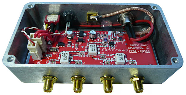
The four SMA sockets that are soldered to the output ports of the PCB also serve as a suitable mount to support the PCB once the sockets are secured in place onto the enclosure. The RF input SMA socket is not directly mounted onto the PCB but connected with a short length of RG316 coax. See image of the completed unit below for clarification!
When using BNC chassis mount sockets, the PCB must be mounted centrally in the base of the diecast box using short PCB pillars and the four mounting holes located on the PCB. The mount holes for the BNC sockets in the diecast box should be carefully measured, placed & drilled so that the centre solder connector pin of each socket lines up with the corresponding input or output pad on the PCB. An earth connection from each of the BNC sockets to the PCB can be made using the BNC sockets earth solder tag.
Here's my Hammond 1590B diecast box drilled and ready for project completion.
Next up is an image of the completed RF Multicoupler built with SMA sockets.
Here's another view from the opposite side, it shows the RF Input socket, DC Power socket, On/Off Switch and status LED.
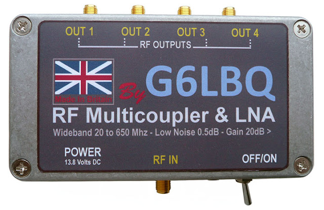
And now the competed project with the lid on and a custom label added that I created in Corel Draw. Looks good, eh :)
So How Does It Perform?
To test the RF Multicoupler, I hooked it up to my spectrum analyser and did a few scans at various frequencies and was surprised to see that the unit is useable down to 1 MHz and as high as 800 MHz with less gain.
I will be using the RF Multicoupler mainly to monitor frequencies between 50 and 460MHz so I did a scan at this range and the result is shown below.
The image shows a reasonably flat trace across the frequency range on test. The spectrum analysers reference level is set to -20dBm so anything above that point is gain produced by the PGA-103+ low noise amplifier. Looking at the trace it can be seen that the gain displayed is between 14 & 19 dBm which is in line with the PGA103+ data sheet after taking into account the losses produced by the combiner splitter parts.
To conclude, I am very happy with the end result of the project, which is now in daily use in the shack. It is worth mentioning that the PGA-103+ LNA device is capable of operating up to 4GHz and alternative splitter/combiners such as the Mini-Circuits ADP-2-20+ could be used to extend the frequency coverage up to 2GHz.
In my next blog post, I continue to work on the Irwell HF Transceiver so keep an eye on the blog for the next instalment!
As usual project files will be made available via the Groups.io platform by joining my G6LBQ community group, where you can discuss my projects, ask questions and help others.
Joining my group is free, just click on the button below.
Until next time...







No comments:
Post a Comment
I appreciate your comments on the blog content, however the blog has been subject to idiots trying to use the comments facility as a means to post advertisements & spam so all comments are now approved and moderated.